FinFET
Latest
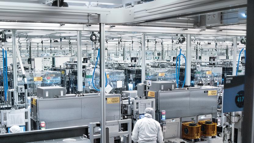
Intel strikes a deal to manufacture MediaTek’s chips
Intel and MediaTek have formed a strategic partnership to build chips for "a range of smart edge devices" using Intel Foundry Services (IFS).

IBM's 2nm transistors matter because of their shape, not size
In the latest "mini" episode of our Upscaled explainer show, we dive into IBM's announcement that it had created 2nm transistors. Size, in this case, isn't the most important innovation.

Intel dishes on Tiger Lake, 'SuperFin' transistors and what lies ahead
Intel has spent the past decade refining its FinFET transistor technology, starting with its Ivy Bridge CPUs in 2012. Now, Intel is ready for its next big architecture leap, SuperFin, its name for a refined FinFET process combined with a "super metal insulator metal capacitor." For users, that mouthful means that Intel has been able to deliver its biggest speed improvement ever within a single node (in this case, its 10 nanometer architecture).

Samsung leapfrogs Intel again with 8-nanometer chips
Samsung has qualified its 8-nanometer chip-making process for production three months ahead of schedule. It's the same "low power plus" (LPP) process used for its current 10-nanometer silicon, not the next-gen extreme ultraviolet (EUV) lithography for its future 7-nanometer tech. That'll yield chips that are ten percent more energy efficient and ten percent smaller than the 10-nanometer ones it's making right now. At the same time, since the 8-nanometer chips use the same process, Samsung will be able to "rapidly ramp up," it said.
Qualcomm's Snapdragon 835 chip is big on photography and VR
Qualcomm hinted that its Snapdragon 835 processor would be something special, and it's ready to show all its cards now that it's at CES, according to a leaked blog post. Battery life is one of the chip's strongest selling points, as you may know (we'll recap that later), but Qualcomm has also revealed that the 835 also carries a ton of upgrades that reflect a rapidly changing mobile landscape. Take virtual reality, for example. On top of 25 percent faster Adreno 540 graphics, it improves positional audio and reduces the lag between motion tracking and what you see on-screen. You won't be as likely to feel seasick or turn the wrong way, in other words.
Qualcomm's Snapdragon 835 is its first 10-nanometer chip
Qualcomm has unveiled its next-gen Snapdragon 835 flagship SoC (system on a chip) and confirmed rumors that it will be built by Samsung using its 10-nanometer FinFET process. Compared to the current 14-nanometer Snapdragon 821 (also built by Samsung), the new processor packs 30 percent more parts into the same space, yielding 27 percent better performance while drawing up to 40 percent less power, the company says. It also improved the design, which will yield "significant" improvements to battery life

MediaTek's octa-core mobile chip focuses on efficiency
Back in June, MediaTek announced its Helio P10 mobile chipset, which will offer octa-core processing and faster LTE to the masses; today, we know that it'll finally be getting into consumers' hands by way of the Sony Xperia XA. So what's next? The Helio P20, of course. Compared to its predecessor, this new chip -- also featuring eight Cortex-A53 cores and LTE Cat 6 -- is a notable upgrade in terms of power efficiency as it'll be fabricated with a 16nm FinFET+ process instead of the old 28nm. For the same reason, the CPU has been allowed to go beyond the old 2GHz limit to 2.3GHz, and the old Mali-T860 GPU has been switched to ARM's cream-of-the-crop Mali-T880 running at 900MHz. As a bonus, the P20 features the same Imagiq image signal processor as the flagship 10-core X20.
Samsung reveals high-end, low-power chips for midrange phones
Samsung has announced that it's bringing its 14nm Exynos chips to cheaper smartphones. These are smaller chips that are both more efficient and more powerful, and given that the company is already putting the technology to use on competitors' chips (namely, Qualcomm's), it's no surprise to see the chip appear in more phones. Until now, Samsung's only put the FinFET-made (that's 3D-structured) 14nm processors in its best -- and most expensive -- phones. That's about to change.

Samsung is making Qualcomm's latest mobile chip
Samsung says it's making new Exynos processors with low-power 14nm chips -- which is no surprise. What is, however, is that the company is also in charge of building Qualcomm's (maker of Snapdragon) latest chips with the same process. Samsung's FinFET 3D structures bump up both performance and reduce power use, which is what makes it ideal for the tiny processors embedded in smartphones. Samsung adds that its second-generation chips improve processor speed by up to 15 percent, and reduce power use by the same amount. Both its homemade Exynos, as well as Qualcomm's chips, have made appearances in Galaxy S phones, but this is the first time Samsung has announced that it would also be making its rivals' chip -- specifically the Snapdragon 820 that's being baked into smartphones now.

AMD's new graphics core is built for laptop gaming
For all the talk of fast graphics in thin laptops, the technology isn't quite there yet. You typically have to choose between a bulky gaming machine and a thin system with pokey low-end video. AMD thinks it might have the cure, however. It just offered a peek at a new graphics architecture, Polaris, that promises gaming-grade performance without the power draw. In Star Wars Battlefront, one of AMD's future chipsets is 61 percent more energy-efficient than a GeForce GTX 950 with similar performance -- in the mobile world, that could make the difference between a slim portable and a big desktop replacement. Even if AMD is cherry-picking the results, this could still lead to speedier visual in laptops and any other small PCs where heat and power are problems.

Here's why the iPad Pro's processor is so fast
Whatever you think of Apple's products, there's little doubt that the A9X processor in the iPad Pro is quick -- in a few cases, it rivals the performance you'd get from a laptop. But why is it so quick, especially when Apple tends to shy away from high clock speeds, many-core processors and other conventional performance tricks? Thanks to AnandTech and Chipworks, we now have a good idea. They've torn down the A9X to reveal that the chip is a series of calculated tradeoffs. It only has two CPU cores and doesn't even have Level 3 memory cache to keep the processor humming, but it has a monstrous amount of bandwidth (51GB per second) and a whopping 12 graphics cores. That's twice as many as in the iPhone 6s' A9 chip, folks. To boot, the A9X is larger than Intel's latest quad-core desktop processors -- Apple has the headroom for components that you don't see in many PCs.

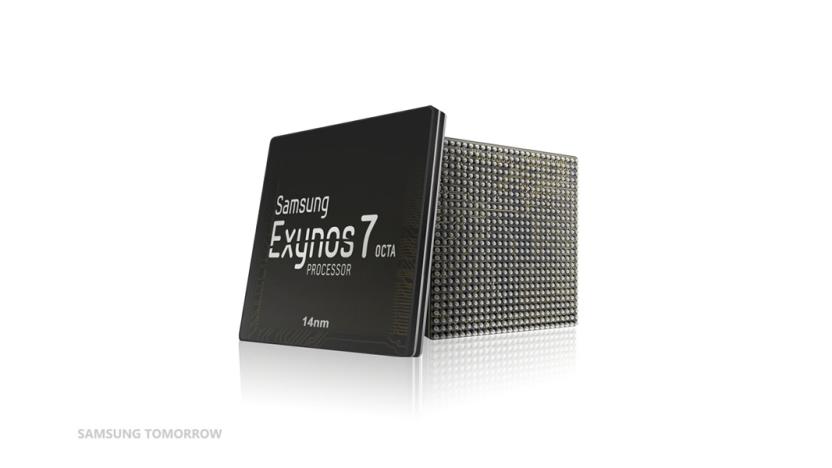
Samsung's 'premium' smartphone chip puts everything in one place
Samsung's next chip is a single square of silicon with a load of things your mobile computer needs. To start, the Exynos 8 Octa 8890 (memorable) is based on 14nm FinFET tech, whose 3D design means better power performance. The company has custom-designed the CPU around a 64-bit ARM design, and will apparently give a 30 percent improvement in performance and ten percent in power efficiency compared to the Exynos 7 Octa it replaces. ARM's Mali-T880 graphics processor also snuggles closely next to a high-end LTE modem. You know, like Qualcomm does.
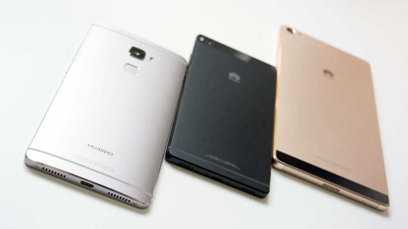
Huawei's next chipset may give competitors a run for their money
Huawei is now Europe's second largest Android brand, according to Kantar, but there's just no time for celebration. Not too long after launching the Huawei Mate S and the Nexus 6P, the Chinese telecom giant is already teasing the launch of the Mate 8 on November 26. Little is known about this new smartphone so far, but it'll likely be using Huawei's upcoming Kirin 950 chipset announced today, which joins the Apple A9 chip to be one of the first to use TSMC's 16nm FinFET Plus process for improved efficiency. Like its predecessor, the Kirin 950 has an octa-core processor but with much improved performance: 4 x Cortex-A72 and 4 x Cortex-A53 instead of the old mid-range offering of just eight Cortex-A53 cores. It also uses ARM's flagship Mali-T880 GPU so gaming should be blast on the phone.

ARM's latest processor design puts fast 4K graphics on your phone
You've probably heard no end of hype for 4K video on TVs and computers, and now it's about to invade your phone... at least, so long as ARM has its way. The company just took the wraps off of Cortex-A72, a processor reference design that promises a huge boost to computing power, especially when graphics come into play. Thanks to updates that include optimizations for an efficient 16-nanometer chipmaking process, 30 percent more memory performance and an 80 percent speedier graphics core (the Mali-T880), the A72 is about 3.5 times more powerful than ARM's earlier Cortex-A15. That's beefy enough to record 4K video at an extra-smooth 120 frames per second -- many current smartphones only manage 30FPS at best. You should get "console-class" gaming, too, and there's a promise of Google Now-style natural voice commands that don't depend on a distant server to interpret what you're saying.

TSMC narrows production of 16nm FinFET chips to late 2013, wants 10nm in 2015
For as often as TSMC has extolled the virtues of FinFET chip designs, we've been wondering exactly when we'd find them sitting in our devices. Thanks to competition from rival semiconductor firms, we'll get them relatively soon: the company now expects to produce its first wave of FinFET-based, 16-nanometer chips toward the end of 2013. While they won't be as nice as 14nm-XM chips in the pipeline, the 16nm parts should still offer battery life and speed improvements over the 28nm chips we know today. These improvements also won't be the end of the road -- TSMC anticipates 10nm designs built on extreme ultraviolet lithography late into 2015, and CEO Morris Chang believes there's seven or more years of advancements in manufacturing before Moore's Law starts breaking down. We'll just be happy if we see FinFET reach our phones and tablets in the near term.

First ARM Cortex-A57 processor taped out by TSMC, ready for fab
Your current smartphone just took another spin backwards on the obsolescence cycle thanks to a new landmark from ARM and TSMC: the first Cortex-A57 has reached the "tape out" stage, meaning it's ready for mass production. The new chip will use TSMC's 16nm FinFET technology (though the transistors will be 20nm for the A57) and will bring up to three times the CPU power of current chips for the same battery life -- or a maximum of five times the battery life at the same speed. The companies said they ramped the chip from design to tape out in a mere six months, though there's no timetable for its arrival in specific devices. When it does start hitting next gen phones and slates though, expect the performance charts to get singed.
Globalfoundries unveils 14nm-XM chip architecture, vows up to a 60 percent jump in battery life
Globalfoundries wants to show that it can play the 3D transistor game as well as Intel. Its newly unveiled 14nm-XM (Extreme Mobility) modular architecture uses the inherently low-voltage, low-leak nature of the foundry's FinFET layout, along with a few traces of its still-in-development 20nm process, to build a 14-nanometer chip with all the size and power savings that usually come from a die shrink. Compared to the larger processors with flat transistors that we're used to, the new technique is poised to offer between 40 to 60 percent better battery life, all else being equal -- a huge help when even those devices built on a 28nm Snapdragon S4 can struggle to make it through a full day on a charge. To no one's shock, Globalfoundries is focusing its energy on getting 14nm-XM into the ARM-based processors that could use the energy savings the most. It will be some time before you find that extra-dimensional technology sitting in your phone or tablet, though. Just as Intel doesn't expect to reach those miniscule sizes until 2013, Globalfoundries expects its first working 14nm silicon to arrive the same year. That could leave a long wait between test production runs and having a finished product in your hands.

ARM and Globalfoundries hammer out deal to promote 20nm mobile chips
Sure it's British, but ARM's mobile empire is being built through careful alliances rather than conquest. The chip designer's latest deal with Globalfoundries, which mirrors a very similar agreement signed with rival foundry TSMC last month, is a case in point. It's designed to promote the adoption of fast, energy-efficient 20nm processors by making it easy for chip makers (like Samsung, perhaps) to knock on Globalfoundries' door for the grunt work of actually fabricating the silicon -- since the foundry will now be prepped to produce precisely that type of chip. As far as the regular gadget buyer is concerned, all this politicking amounts to one thing: further reassurance that mobile processor shrinkage isn't going to peter out after the new 32nm Exynos chips or the 28nm Snapdragon S4 -- it's going to push on past the 22nm benchmark that Ivy Bridge already established in the desktop sphere and hopefully deliver phones and tablets that do more with less juice.

ARM and TSMC team up on 64-bit chips and FinFET transistors
ARM and TSMC are renewing their vows and plan to continue collaborating well into the future, as they work to optimize the 64-bit v8 architecture for the Taiwanese company's FinFET transistor tech. The two will push next-gen ARM chips to 20nm and beyond, and hopefully shorten the time to market for new designs. The FinFET process should also help boost frequencies, while keeping power consumption low -- a key to the continued success of the RISC architecture. The FinFET architecture is similar to Intel's own tri-gate transistor technology that was instrumental to nudging the Core architecture forward with Ivy Bridge. After those 64-bit ARM chips are up and running at 20nm and powering your next-gen smartphone, TSMC will begin to look at even smaller processes, with an eye on 15nm next. You'll find the entire joint profession of their love for one another after the break.

Intel going 3D for future CPUs
Seems like everything's going 3D these days. Thanks a lot, James Cameron. Now even Intel's getting in on the act, but in a manner that sounds like it has more useful applications than the latest Sony TVs or Nintendo's 3DS. As a bonus, you also don't have to wear any goofy-looking glasses. The New York Times reports Intel has developed a technology called Finfet (or fin field-effect transistor) that will allow Intel to manufacture three-dimensional CPUs. Until now, the conductive area of the transistors used in CPUs has been two-dimensional, which means that in order to pack a higher number of transistors within the same space, the transistors had to shrink to smaller sizes. Over the years, manufacturing tolerances have traditionally been the limiting factor in how small a transistor can get, but these CPU building blocks are now approaching a size where physics itself becomes a barrier to making them any smaller. Intel's Finfet aims to work around this problem by building "fins" into the transistor structure, making the transistor's conductive area three-dimensional. Intel expects chips using this design to be 37 percent faster than current low-voltage chips while consuming half the power. Not all chipmakers are convinced that going 3D is the right solution, and a few of them are taking a "wait and see" approach to Intel's Finfet technology. Intel plans to start producing chips using Finfet later this year, but there's obviously no indication yet when or even if chips using Finfet will find their way into future Macs. Intel's also admitted that the consumer "ecosystem" isn't a favorable market for Intel today, which may mean the chipmaker has its eye on crafting a Finfet-based competitor (or replacement) for Apple's A-series chips used in iOS devices.


