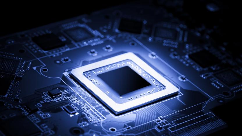
MooresLaw
Latest

Magnetized particles could solve our data storage problems
Scientists have discovered an unusual magnetic behavior that could solve one of the biggest problems faced by our data-hungry world: data storage. In recent decades we've been getting progressively better at storing data but unless we find new and more efficient ways to store the increasing volume of data we're producing every day, it won't be long until data centres reach their capacities and progress grinds to a halt. The new discovery, which has the potential to store data in fast-moving magnetic particles, could remedy that.
Super-thin semiconductors delay the 'death' of silicon
Silicon has been the backbone of processors for decades, but it's rapidly approaching its physical limits: making a chip on a process smaller than 5 nanometers is usually impossible without introducing problems. How is Moore's Law for chip complexity going to survive? Stanford researchers have a solution: augment it with materials that outdo silicon where it counts. They've pinpointed two semiconductors, hafnium diselenide and zirconium diselenide, that can be made extremely thin (just three atoms thick) while self-insulating far more effectively than silicon. You could get transistors that are 10 times smaller than the smallest you get from silicon alone -- 5nm chips would seem bloated compared to what's possible with these diselenides.
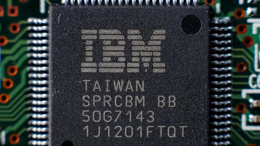
IBM squeezes 30 billion transistors into a fingernail-sized chip
Who said Moore's Law was dead? Certainly not IBM or its chip partners Globalfoundries and Samsung. The trio has developed a transistor manufacturing process that should pave the way for 5-nanometer chips. While the team etched the chip using the same extreme ultraviolet lithography (EUV) used for the breakthrough 7nm chip, it ditched the common FinFET (fin field effect) transistor design in favor of stacks of silicon nanosheets. The switch makes it possible to fine-tune individual circuits to maximize their performance as they're crammed into an incredibly small space. How small? At 5nm, the group says it can squeeze 30 billion transistors into a chip the size of a fingernail (see below) -- not bad when the 7nm chip held 20 billion transistors a couple of years ago.
Self-assembling wires could lead to faster processors
There's a very real fear that processor speed upgrades will slow to a crawl as it becomes increasingly difficult to make denser chips. Don't tell that to a team of researchers at MIT and in Chicago, though -- they've devised a chip-making technique that could keep Moore's Law relevant for a while longer. Their approach produces much finer wires by letting them partly assemble themselves, rather than relying on the very deliberate (not to mention slow) ultraviolet or scanning processes used to make chips today.
Intel: Our next chips will be a 'generation ahead' of Samsung
Intel says that when its long-delayed 10-nanometer Cannon Lake chips finally arrive, they'll be a "full generation ahead" of rivals Samsung and TMSC, thanks to "hyper scaling" that squeezes in twice as many transistors. That will yield CPUs with 25 percent more performance and 45 percent lower power use than its current Kaby Lake chips when they ship towards the end of 2017. Furthermore, Intel thinks the tech will keep Moore's Law going and give it a 30 percent cost advantage over competitors like AMD.
Researchers think chaos theory can get us past Moore's Law
Gordon Moore, co-founder of Intel, believed that the number of transistors on an integrated circuit would double every year or two. And, to his credit, that rule pretty much held out between 1965 and 2015, when the laws of physics began to get in the way. Now, researchers at North Carolina State believe that we don't need to obsess over ever-smaller transistors to make chips even more powerful. Instead, they've turned to chaos theory in the hope that mixing things up will provide the performance boost that Intel can't.

Roadmap says transistors will stop shrinking in 5 years
Whether or not Moore's Law on complexity has always held true, you've had one constant in the semiconductor world: chip makers would always find a way to shrink transistors and create more powerful chips without increasing size or power consumption. However, even that one hint of predictability might soon disappear. The Semiconductor Industry Association (which includes the likes of IBM and Intel) has published a roadmap which expects transistors to stop shrinking after 2021. Simply speaking, it might not be financial practical to keep reducing transistor sizes -- companies might not recoup the costs. Instead, they may focus on 3D chips an other technologies that make better use of available space.

Intel is officially slowing down the pace of CPU releases
To make consumers crave its next generation of CPUs, Intel has produced chips on a yearly tick-tock cycle for the last decade. Thanks to the shrinking die sizes, that process may permanently become a three-step, according to financial documents spotted by Motley Fool. The company has already had significant issues going from 22- to 14-nanometers, and it extended the latter to a third generation with "Kaby Lake" chips. That was the first break from tick-tock, but Intel has now confirmed that the longer rhythm, which it calls "process, architecture, optimization (PAO)" will continue for its upcoming 10-nanometer chips.

Moore's Law in action: making our machines ever more micro
Over the past few decades, engineers have leveraged Moore's Law to the fullest, resulting in powerful ultrathin laptops and feature-rich miniature wearables. Back in 1981, a 23-pound Osborne 1 computer was considered portable, with 64KB of onboard memory. Today, smartphones weigh just a few ounces and easily pack 128GB of storage. There's also a vastly more complex architecture of circuits and sensors inside these devices, all at a scale nearly invisible to the eye. It's taken us decades to develop and shrink down these microelectronics to where they are today, which is no small feat. Join us as we ride the ever-shrinking gadget wave from its early days to some of the nanoscopic creations at work today.

The law that predicts computing power turns 50
Today represents a historic milestone in technology: It's the 50th anniversary of Moore's Law, the observation that the complexity of computer chips tends to double at a regular rate. On April 19th, 1965, Fairchild's Gordon Moore (later to co-found Intel) published an article noting that the number of components in integrated circuits had not only doubled every year up to that point, but also would continue at that pace for at least a decade. He would later revise that guideline to every two years, but the concept of an unofficial law of progress stuck. It not only foresaw the rapid expansion of computing power, but also frequently served as a target -- effectively, it became a self-fulfilling prophecy.

TSMC narrows production of 16nm FinFET chips to late 2013, wants 10nm in 2015
For as often as TSMC has extolled the virtues of FinFET chip designs, we've been wondering exactly when we'd find them sitting in our devices. Thanks to competition from rival semiconductor firms, we'll get them relatively soon: the company now expects to produce its first wave of FinFET-based, 16-nanometer chips toward the end of 2013. While they won't be as nice as 14nm-XM chips in the pipeline, the 16nm parts should still offer battery life and speed improvements over the 28nm chips we know today. These improvements also won't be the end of the road -- TSMC anticipates 10nm designs built on extreme ultraviolet lithography late into 2015, and CEO Morris Chang believes there's seven or more years of advancements in manufacturing before Moore's Law starts breaking down. We'll just be happy if we see FinFET reach our phones and tablets in the near term.

MIT researchers concoct smallest indium gallium arsenide transistor ever made
Researchers at MIT's Microsystems Technology Laboratories may be giving Moore's Law a new lease on life with the development of the smallest indium gallium arsenide transistor ever made, measuring up at 22-nanometers. Such transistors could produce more current when shrunken down than those based on silicon, which means chips may continue to pack in more transistors while providing a bigger punch. "We have shown that you can make extremely small indium gallium arsenide MOSFETs (metal-oxide semiconductor field-effect transistors) with excellent logic characteristics, which promises to take Moore's Law beyond the reach of silicon," says co-developer of the tech Jesús del Alamo. The development is an encouraging step in the right direction, but the MIT team still has a long road ahead of it before the tech shows up in your gadgets. Next on the docket for the scientists is improving the transistor's electrical performance and downsizing it to below 10-nanometers. For the nitty gritty on how the transistor was built, hit the adjacent source link.

ARM chief tosses Moore's Law out with the trash, says efficiency rules all
ARM CEO Warren East already has a tendency to be more than a bit outspoken on the future of computing, and he just escalated the war of words with an assault on the industry's sacred cow: Moore's Law. After some prompting by MIT Technology Review during a chat, East argued that power efficiency is "actually what matters," whether it's a phone or a server farm. Making ever more complex and power-hungry processors to obey Moore's Law just limits how many chips you can fit in a given space, he said. Not that the executive is about to accept Intel's position that ARM isn't meant for performance, as he saw the architecture scaling to high speeds whenever there was a large enough power supply to back it up. East's talk is a bit long on theory and short on practice as of today -- a Samsung Chromebook isn't going to make Gordon Moore have second thoughts -- but it's food for thought in an era where ARM is growing fast, and even Microsoft isn't convinced that speed rules everything.

Acronym-loving Samsung joins Intel and TSMC, buys stake in ASML
Samsung's round of cash-flashing continues with a $629 million purchase of a three-percent stake in ASML. It's joining Intel and TSMC in pumping money into the Dutch business, developing tooling for chip-making machines with Extra Ultraviolet Lithography (EUV) designed to "extend Moore's Law." It'll also help reduce the cost of future silicon, since it'll enable the companies to use wider silicon wafers along the manufacturing line. Given that Samsung's investment caps of a project to raise nearly $5 billion in cash and that ASML's home is just five miles west of PSV Eindhoven's stadium, we just hope they threw in a few home tickets for their trouble.

Researchers take nanowire transistors vertical, double up on density
3D silicon is all the rage, and now nanowire transistors have further potential to keep Moore's Law on life support. Researchers at A*STAR have found a way to double the number of transistors on a chip by placing the atomic-scale wires vertically, rather than in the run-of-the-mill planar mode, creating two "wrap-around gates" that put a pair of transistors on a single nanowire. In the future, the tech could be merged with tunnel field effect transistors -- which use dissimilar semiconductor materials -- to create a markedly denser design. That combo would also burn a miniscule percentage of the power required conventionally, according to the scientists, making it useful for low-powered processors, logic boards and non-volatile memory, for starters. So, a certain Intel founder might keep being right after all, at least for a few years more.

Engadget Primed: why nanometers matter (and why they often don't)
Primed goes in-depth on the technobabble you hear on Engadget every day -- we dig deep into each topic's history and how it benefits our lives. You can follow the series here. Looking to suggest a piece of technology for us to break down? Drop us a line at primed *at* engadget *dawt* com. Welcome to one of the most unnecessarily complicated questions in the world of silicon-controlled gadgets: should a savvy customer care about the underlying nature of the processor in their next purchase? Theoretically at least, the answer is obvious. Whether it's a CPU, graphics card, smartphone or tricorder, it'll always receive the Holy Grail combo of greater performance and reduced power consumption if it's built around a chip with a smaller fabrication process. That's because, as transistors get tinier and more tightly packed, electrons don't have to travel so far when moving between them -- saving both time and energy. In other words, a phone with a 28-nanometer (nm) processor ought to be fundamentally superior to one with a 45nm chip, and a PC running on silicon with features etched at 22nm should deliver more performance-per-watt than a 32nm rival. But if that's true, isn't it equally sensible to focus on the end results? Instead of getting bogged down in semiconductor theory, we may as well let Moore's Law churn away in the background while we judge products based on their overall user experience. Wouldn't that make for an easier life? Well, maybe, but whichever way you look at it, it's hard to stop this subject descending into pure philosophy, on a par with other yawnsome puzzles like whether meat-eaters should visit an abattoir at least once, or whether it's better to medicate the ailment or the person. Bearing that in mind, we're going to look at how some key players in the silicon industry treat this topic, and we'll try to deliver some practical, offal-free information in the process.

Raspberry Pi hands-on and Eben Upton interview at Maker Faire (video)
Unless you've been hiding under a rock lately, we're pretty sure you've heard about the Raspberry Pi by now -- a $25 credit-card sized PC that brings ARM/Linux to the Arduino form factor. As a refresher, the system features a 700MHz Broadcom BCM2835 SoC with an ARM11 CPU, a Videocore 4 GPU (which handles HD H.264 video and OpenGL ES 2.0) and 256MB RAM. The board includes an SD card slot, HDMI output, composite video jack, 3.5mm audio socket, micro-USB power connector and GPIO header. Model A ($25) comes with one USB port, while Model B ($35) provides two USB ports and a 100BaseT Ethernet socket. Debian is recommended, but Raspberry Pi can run most ARM-compatible 32-bit OSes. This past weekend at Maker Faire Bay Area 2012 we ran into Eben Upton, Executive Director of the Raspberry Pi Foundation, and took the opportunity to spend some quality time with a production board and to discuss this incredible PC. We touched upon the origins of the system (inspired by the BBC Micro, one of the ARM founders' projects), Moore's law, the wonders of simple computers and upcoming products / ideas -- including Adafruit's Pi Plate and Raspberry Pi's prototype camera add-on. On the subject of availability, the company expects that "there will be approximately 200,000 units in the field by the end of June". Take a look at our hands-on gallery below and our video interview after the break.%Gallery-155800%

Single atom transistors point to the future of quantum computers, death of Moore's law
Transistors -- the basic building block of the complex electronic devices around you. Literally billions of them make up that Core i7 in your gaming rig and Moore's law says that number will double every 18 months as they get smaller and smaller. Researchers at the University of New South Wales may have found the limit of this basic computational rule however, by creating the world's first single atom transistor. A single phosphorus atom was placed into a silicon lattice and read with a pair of extremely tiny silicon leads that allowed them to observe both its transistor behavior and its quantum state. Presumably this spells the end of the road for Moore's Law, as it would seem all but impossible to shrink transistors any farther. But, it could also points to a future featuring miniaturized solid-state quantum computers.

IBM builds 9 nanometer carbon nanotube transistor, puts silicon on notice
It's not the smallest transistor out there, but the boffins at IBM have constructed the tiniest carbon nanotube transistor to date. It's nine nanometers in size, making it one nanometer smaller than the presumed physical limit of silicon transistors. Plus, it consumes less power and is able to carry more current than present-day technology. The researchers accomplished the trick by laying a nanotube on a thin layer of insulation, and using a two-step process -- involving some sort of black magic, no doubt -- to add the electrical gates inside. The catch? (There's always a catch) Manufacturing pure batches of semiconducting nanotubes is difficult, as is aligning them in such a way that the transistors can function. So, it'll be some time before the technology can compete with Intel's 3D silicon, but at least we're one step closer to carbon-based computing.

IBM sees stacked silicon sitting in fluid as the way to power future PCs
Generally, the combination of microchips, electricity and fluids is usually considered an incredibly bad thing. IBM, however, thinks it can combine those three to make super small and super powerful computers in the future. The idea is to stack hundreds of silicon wafers and utilize dual fluidic networks between them to create 3D processors. In such a setup, one network carries in charged fluid to power the chip, while the second carries away the same fluid after it has picked up heat from the active transistors. Of course, 3D chips are already on the way, and liquid cooled components are nothing new, but powering a PC by fluids instead of wires has never been done before. Bruno Michel, who's leading Big Blue's research team, has high hopes for the technology, because future processors will need the extra cooling and reduced power consumption it can provide. Michel says he and his colleagues have demonstrated that it's possible to use a liquid to transfer power via a network of fluidic channels, and they to plan build a working prototype chip by 2014. If successful, your smartphone could eventually contain the power of the Watson supercomputer. Chop, chop, fellas, those futuristic fluidic networks aren't going to build themselves.


