Intel seems pretty excited about glass substrates
They'll help Intel build denser and more efficient chips.
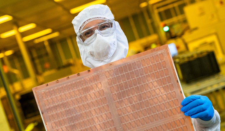
These days when we talk about what's next for chip design, we focus on things like cramming in more cores, increasing clock speeds, shrinking transistors and 3D stacking. We rarely think about the package substrate, which holds and connects those components. Today Intel, in the midst of its reinvention as a foundry company, has announced it's made a major breakthrough in substrate materials—and it's all about glass.
The company says its new glass substrate, which is set to arrive in advanced chip designs later this decade, will be stronger and more efficient than existing organic materials. Glass will also allow the company to cram more chiplets and other components next to each other, something that could lead to flexing and instability with an existing silicon package using organic materials.
"Glass substrates can tolerate higher temperatures, offer 50% less pattern distortion, and have ultra-low flatness for improved depth of focus for lithography, and have the dimensional stability needed for extremely tight layer-to-layer interconnect overlay," Intel said in a press release. With these capabilities, the company claims glass substrates will also lead to a ten-fold increase in interconnect density, as well as allow for "ultra-large form-factor packages with very high assembly yields."
We're slowly beginning to see what Intel's future chips could actually look like. Two years ago, the company announced its "gate-all-around" transistor design, RibbonFET, as well as PowerVia, which would let Intel move power delivery to the rear of a chip wafer. At the same time, Intel also announced it would be building chips for Qualcomm and Amazon's AWS service.
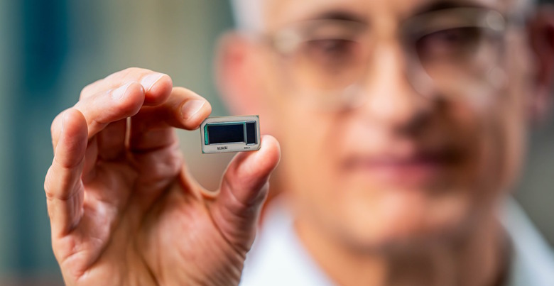
Intel says we'll see chips using glass substrates in areas in high performance areas first, like AI, graphics and data centers. The glass breakthrough is another sign that Intel is ramping up its advanced packaging capabilities for its US foundries, as well. That's something TSMC is reportedly stumbling on with its Phoenix, Arizona plant, which will require shipping chip materials back to Taiwan for advanced packaging.