Electron microscope draws nano-sized patterns in metal ink
The breakthrough could lead to finely detailed, super-optimized electronics.
One of the greatest challenges in designing electronics is drawing very fine details. You normally need lithography, which complicates the process by requiring masks. However, Oak Ridge National Laboratory has now found a way to write at an extremely fine level — and even get a little bit creative. Its researchers have developed a technique that relies on an electron microscope to draw nanoscale patterns using metal ink. The team first creates a grayscale template to guide its work, and uses the microscope to shoot electrons into palladium chloride cells along that template. The cells neatly deposit raw palladium wherever the microscope goes.
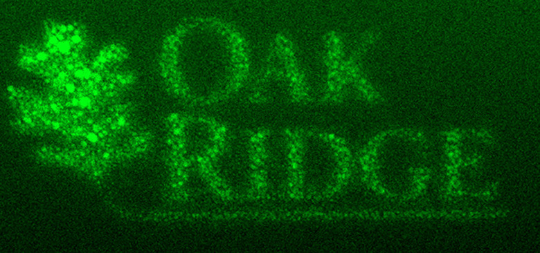
If you want to fine-tune your output, you only have to control the microscope's speed and electron volume. And even in this early testing, the results are highly accurate: as you can see above, Oak Ridge managed to create an extremely tiny version of its own logo.
There's still a long way to go before the technology is ready for prime time. The lab wrote at a resolution of 40 nanometers, while the processors in many modern PCs and phones are built on a 14-nanometer process. When it's ready, however, it could help craft highly optimized electronics that aren't practical using existing manufacturing methods.