1
Another parent has filed a wrongful death suit against OpenAI
Yet another parent is suing OpenAI, claiming its chatbot did not do enough to prevent their child's death by suicide.
Read More
Yet another parent is suing OpenAI, claiming its chatbot did not do enough to prevent their child's death by suicide.
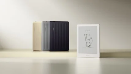
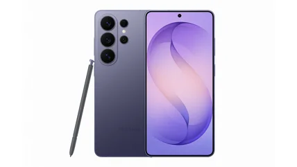
Read MoreBoox's new Go 6 ereader offers stylus support for note-taking.
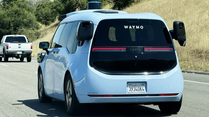
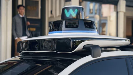
Read MoreWaymo will happily relieve you of $30 a month in exchange for not a whole lot.
Read MoreThe Philips Skylight recreates natural daylight indoors, but we may not be able to buy it in the US.
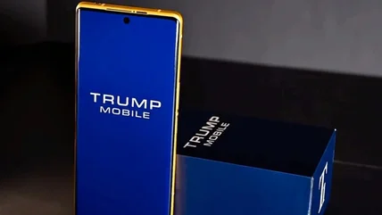
Read MoreThe only functional difference between a Trump Phone and the HTC U24 Pro is the battery, iFixit discovered.
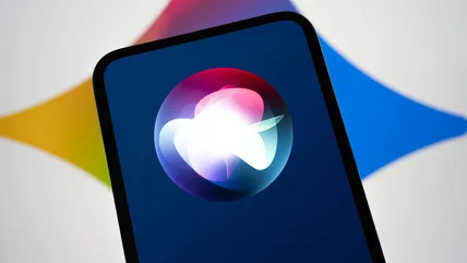
Read MoreApple is more focused on delivering usable features with Siri AI, instead of hyping up agentic AI. That's a good thing.
Read MoreBluesky is launching a communities feature this year, according to its head of product.
Read MoreFramework is pushing back shipments of its new Laptop 13 Pro to address issues with its haptic touchpad and display found in the run-up to mass production.
Read MoreAnthropic is walking back a hidden policy that researchers say sabotaged their work.
Read MoreOpenAI has published a report detailing how China-linked influence campaigns against data centers used ChatGPT.
Read MoreThe update brings a low-latency profile, speeds up search, and patches hundreds of flaws.
Read MoreThe regulation also imposes new safety expectations on 'AI chatbot services.'
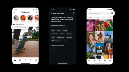
Read MoreInstagram has expanded its algorithm personalization features to its main feed.
Read MoreThe UK's communications regulator has reminded social media platforms they have a duty to minimize hateful content, not encourage it.
Read MoreWe dive into our initial thoughts on Siri AI and Tim Cook's legacy.
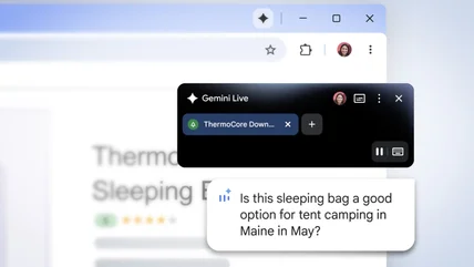
Read MoreGemini in Chrome continues to roll out and has now landed in Latin America, the Middle East and Africa.
Read MoreMicrosoft Office 2019 for Mac will effectively become useless next month.
Read MoreIf you've ever needed iPad data for a day or two without signing a contract or paying for an entire month, AT&T has a new option.
Read MoreIt’s actually a security feature.
Read MoreInsta360 has launched its first gimbal camera, the $770 Luna Ultra.
Read MoreWaymo made a virtual driver called ReD to help its robotaxis avoid accidents.
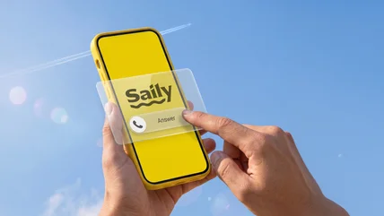
Read MoreYou now can get a US phone number with NordVPN’s Saily eSIM app.
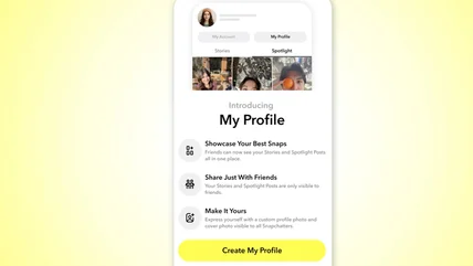
Read MoreMaybe it wasn't a great idea to let 14-year-olds post videos to Spotlight in the first place.
Read MoreThe Seattle City Council has approved a moratorium on the construction of large data centers.
Read MoreAt long last, a corporate training you might actually enjoy.
Read MoreThe rules may pose a minor hurdle for people who just have to cheat.
Read More