0
OpenAI will provide free AI models to select researchers
The program, ChatGPT for Academic Researchers, will start with 10,000 participants this summer.
Read More
The program, ChatGPT for Academic Researchers, will start with 10,000 participants this summer.
Read MoreWaymo paused highway operations in May after several robotaxis drove into sections that were closed for construction.
Read MoreMoving your data to Claude is easier than you might think. This step-by-step guide will get you switched over right away.
Read MoreWe played spot the difference and noticed this intriguing difference in Google's teaser for the Pixel 11 Pro.
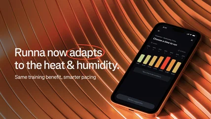
Read MoreIf it's extra hot or humid where you are, the Runna app will adjust your workouts accordingly.
Read MoreX and the World Federation of Advertisers say they're resetting their relationship.
Read MoreIt's a widely held belief that restarting your phone improves performance. Here's the truth.
Read MoreThe company developed the DoorDash Air drones in-house.
Read MoreUsers only have to long-press the ‘fn’ key on the bottom left corner of their keyboard to talk to Gemini on Mac.
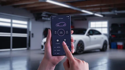
Read MoreSome newer vehicles include the feature, but to keep it, you'll have to pay monthly. You can also buy remote starters outright.
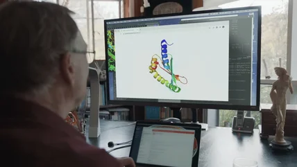
Read MoreDeepMind's award-winning AlphaFold team is no more.
Read MoreOpenAI’s investigation starts shedding light on the activities of its rogue agent that hacked Hugging Face.
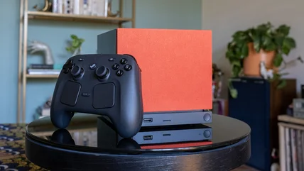
Read MoreValve says that no one on its Steam Machine waitlist is leapfrogging over anyone currently holding a reservation.
Read MoreElon Musk’s xAI has filed a lawsuit to block Minnesota’s new law that would ban apps that can generate nonconsensual intimate imagery from being enforced.
Read MoreIt's part of a national security strategy to kickstart domestic production of emerging technology.
Read MoreIna and David Steiner will receive compensation after a 2019 campaign to silence their critiques of the company.
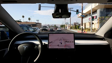
Read MoreA new lawsuit accuses Tesla of overextending the safety operators overseeing its robotaxis.
Read MoreA thousand workers from OpenAI, Anthropic, Google, Meta and more have signed the letter.
Read MoreIf you've got an older iPhone hanging out in the junk drawer, grab it out and bring it back to life with these tips.
Read MoreDon't worry, the Trump administration won't let a little acid rain get in the way of more data centers.
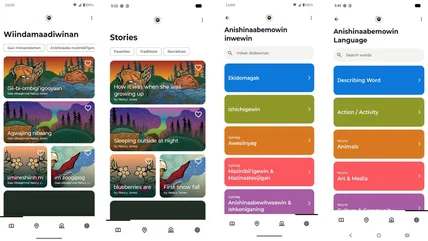
Read MoreThe free Android app shares knowledge from members of the Rainy Lake Ojibwe community.
Read MoreApple's new program gives you lease options for iPhone, iPad, Apple Watch and Mac.
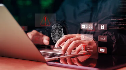
Read MoreResearchers investigating Hugging Face found the majority of its models would generate non-consensual deepfakes.
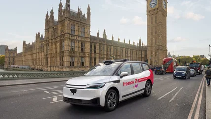
Read MoreAs it promised last year, Baidu has started testing its robotaxis in London along with partners Lyft and Freenow.
Read MoreChatGPT has been refusing to imitate the writing of famous authors, both living and dead.
Read MoreHere's what the rumor mill tells us Google might be preparing for its next Pixel launch.
Read More