0
NordVPN’s Saily eSIM offers a US phone number for $1 a month
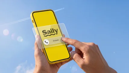
You now can get a US phone number with NordVPN’s Saily eSIM app.
Read More
You now can get a US phone number with NordVPN’s Saily eSIM app.
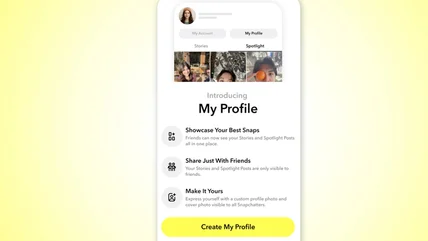
Read MoreMaybe it wasn't a great idea to let 14-year-olds post videos to Spotlight in the first place.
Read MoreThe Seattle City Council has approved a moratorium on the construction of large data centers.
Read MoreAt long last, a corporate training you might actually enjoy.
Read MoreThe rules may pose a minor hurdle for people who just have to cheat.
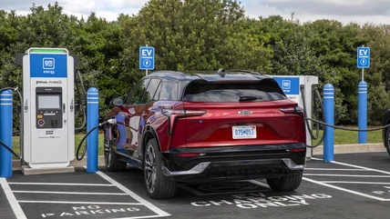
Read MoreEVs from GM will soon be able to top up at more kinds of public chargers.
Read MoreClaude subscribers can try the model until June 22 without spending usage credits.
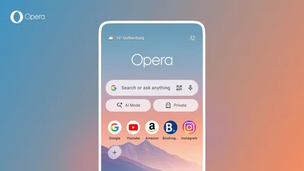
Read MoreOpera's new Android update includes a soccer hub in time for the World Cup.
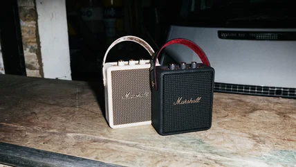
Read MoreMarshall's Stockwell III portable speaker runs 40 hours on a charge and costs $250.
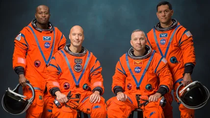
Read MoreNASA has announced the crew of its critical Artemis III.
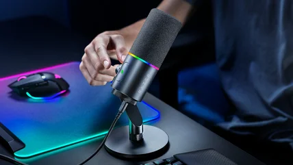
Read MoreA podcast and streaming ready microphone for all skill levels, and yes, it has RGB.
Read MoreWill Siri AI actually be useful, or is it more AI marketing fluff? We chat about that, and everything else Apple announced at its WWDC 2026 keynote, on the Engadget Podcast.
Read MoreBeta versions of iOS, iPadOS and watchOS are available to download if you have a developer account.
Read MoreIt's not perfect, but Rivian's latest shows this company is playing for keeps.
Read MoreThe Defense Department has released an updating list of companies linked to the Chinese military, and it now includes Alibaba and Baidu.
Read MoreThe FCC has given Amazon an extension to a key milestone for its Leo satellite internet deployment.
Read MoreYou can now rearrange posts on Instagram the way you want to.
Read MoreCan’t a multi-trillion-dollar company have secrets any more?
Read More"We expect it to leak so we're just announcing it."
Read MoreThe AI subscription now starts at $5 per month.
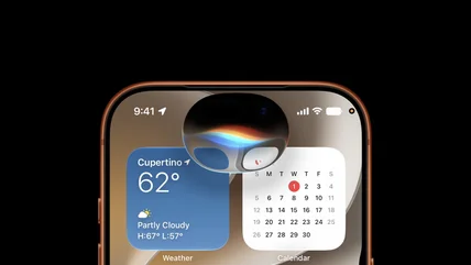
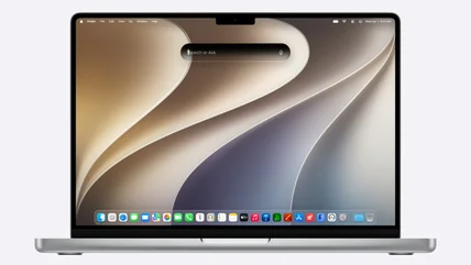
Read MoreApple's focus on efficiency and performance improvements is good news for older iPhones.
Read MoreYou’ll need to be running Apple silicon to use the latest operating system.
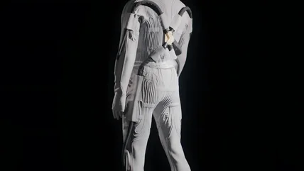
Read MoreAxiom has showed off its new spacesuit's inner layer, designed to keep astronauts cool on the moon.
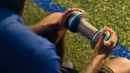
Read MoreThe CryoTherm Palm can switch between cold, heat and contrast therapy.
Read MoreThe revamped AI tool will roll out in the coming weeks, according to The Financial Times.
Read MoreDetails for a potential deal haven’t been finalized yet.
Read MoreThe memo also prevents companies from altering AI models being used by the military without prior approval.
Read More