0
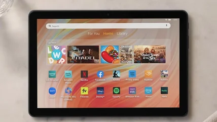
International Google Pixels are different than American models - here's how
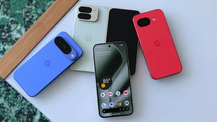
In case you were wondering in which country you should buy a Pixel phone, you world traveler you.
Read More
In case you were wondering in which country you should buy a Pixel phone, you world traveler you.
Read MoreA RAM upgrade? In this memory economy?!
Read MoreThis week on the Engadget Podcast, we've got our first impressions of Valve's pricey Steam Machine, and we chat about Sony dumping PlayStation discs in 2028.
Read MoreGet ready to navigate a free-for-all of social media handles.
Read MoreSony is converting its PlayStation disc factory into a plant for optical microlenses.
Read MoreTesla has started taking orders for the Model Y Long Wheelbase in the US and Puerto Rico.
Read MorePocket is listed in app stores but seemingly unavailable in the US.
Read MoreThe hosting platform wants sites to have more control over how AI companies use their content.
Read MoreLaptop chargers are much easier to travel with these days, and there's one specific technology that is largely to thank.
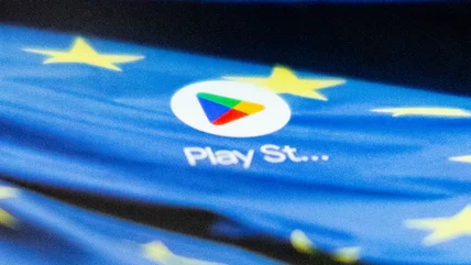
Read MoreThe company has been gaining traction in Europe.
Read MoreThere are now enough Amazon Leo satellites to launch the service, but its constellation is still tiny compared to Starlink’s.
Read MoreA long-defunct developer returned from the dead promising to revive the 3DO, but quickly pulled its pledge when it became apparent it didn't have the right to.
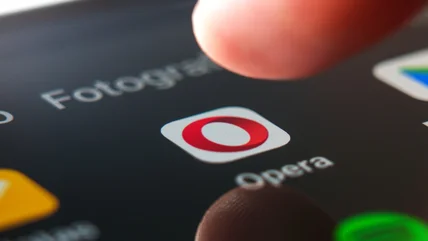
Read MoreOpera has introduced a new safety feature that protects against malicious 'ClickFix' clipboard attacks.
Read MoreAccording to the Financial Times, Sam Altman is floating the idea of having leading AI companies give US sovereign funds a five percent equity.
Read MoreEurope's highest court of appeal has upheld a record-setting $4.7 billion fine imposed on Google back in 2018.
Read MoreX has launched a new live streaming command center and additional creator payouts.
Read MoreNext spring could be a fiesta of new iPads, MacBooks and iPhones.
Read MoreMusk has debunked reports that a rumored SpaceX device could offer a way to access xAI's models without having to use a smartphone.
Read MoreFar-UVC could help rid future cars of odors.
Read MoreIf you really want to get retro, Fujifilm is making some special editions of its classic instant camera.
Read MoreUN panel says ‘AI is neither inherently good nor bad,’ but better safeguards around it are needed.
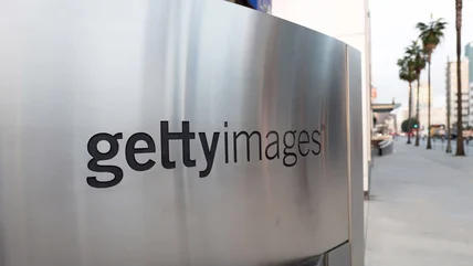
Read MoreGetty Images has moved to terminate a $3.7 billion merger with rival Shutterstock due to restrictions imposed by UK regulators.
Read MoreBMW's X5 lineup finally has an electric option with impressive range.
Read MoreMeta’s Conversation Focus feature for smart glasses is now only free for three hours a month.
Read MoreThe Gemini macOS app now has access to Google’s Spark agentic AI assistant.
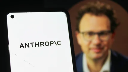
Read MoreAnthropic will start its users’ access to Mythos and Fable tomorrow, July 1.
Read MoreAnthropic trained its newest Sonnet model to excel at agentic tasks, which have been causing a headache for the company's enterprise customers and power users.
Read More