semiconductor
Latest

Toyota forms a joint venture to make its own self-driving car chips
Toyota is getting into the semiconductor business, partnering with auto supplier Denso to form a new company focused on chip manufacture.
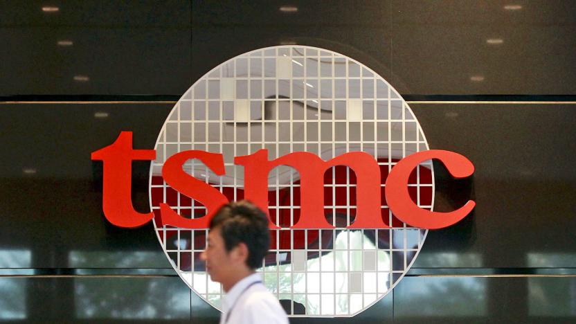
Chip giant TSMC struggles with virus infections at its factories
Many of the tech products launching this fall might have just run into production setbacks. Giant chip manufacturer TSMC has warned that several of its fabrication plants suffered virus infections on August 3rd, disrupting production. Some of these plants recovered in a "short period of time," it said, but others wouldn't resume business as usual for "one day." The company dismissed claims that this was a hack, but didn't initially provide details about the virus or the potential infection path.
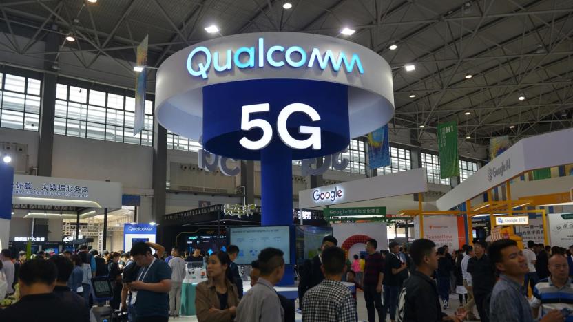
Qualcomm gives up on buying chip giant NXP
Qualcomm has been trying to buy giant chip maker NXP for the better part of two years. All that patience might not have paid off, however. Qualcomm is planning to drop its bid for NXP by the end of July 25th (that's today, if you're reading in time). Its executives reportedly expect Chinese regulators to shoot down the deal, with CEO Steve Mollenkopf pinning it partly on the "current geopolitical environment." In other words, Trump's trade war with China is dimming what chances were left of a merger.

Toshiba's chip drama ends with sale to a financial group
The long-running bidding war over Toshiba's flash memory business has effectively come to an end... and the winner probably isn't who you expected. Toshiba has agreed to sell its NAND division to a group led by the private equity firm Bain Capital for the equivalent of $18 billion. This isn't going to please Western Digital, Toshiba's partner in the US, but Toshiba expects the deal to survive any legal battles. The question is why -- and whether or not Toshiba's eagerness to sell might cost you in the long run.
Super-thin semiconductors delay the 'death' of silicon
Silicon has been the backbone of processors for decades, but it's rapidly approaching its physical limits: making a chip on a process smaller than 5 nanometers is usually impossible without introducing problems. How is Moore's Law for chip complexity going to survive? Stanford researchers have a solution: augment it with materials that outdo silicon where it counts. They've pinpointed two semiconductors, hafnium diselenide and zirconium diselenide, that can be made extremely thin (just three atoms thick) while self-insulating far more effectively than silicon. You could get transistors that are 10 times smaller than the smallest you get from silicon alone -- 5nm chips would seem bloated compared to what's possible with these diselenides.

Samsung's high-capacity V-NAND memory is perfect for massive SSDs
Just over four years since it unveiled the first 3D vertical NAND memory, Samsung has developed its first 1 terabit (Tb) V-NAND chip. The flash memory technology, used in devices ranging from smartphones to digital cameras, will launch next year. As its name suggests, V-NAND boasts a vertically stacked structure with greater density than memory cells placed on a single, 2D plane. The result is more speed, up to ten times more reliability, and less chance of a breakdown. As with its 256 gigabit consumer SSDs, Samsung's new chips will probably find their way into your next laptop, and maybe even future phones. That's not all, Samsung also announced that the 1Tb chip will enable a single V-NAND package with 2 terabytes of memory capacity. As you might have guessed, that could mean more bang for your buck when it comes to SSDs for home PCs.

Samsung topples Intel as world’s largest chipmaker
Samsung registered a record profit of $12.6 billion in its second quarter earnings report, but hidden in those numbers lies another milestone. Of its $54 billion in revenue, $15 billion came solely from Samsung Semiconductors -- pushing it above the $14.8 billion that all of Intel brought in. In short: Samsung just ended Intel's 24-year-reign and became the largest chipmaker in the world.
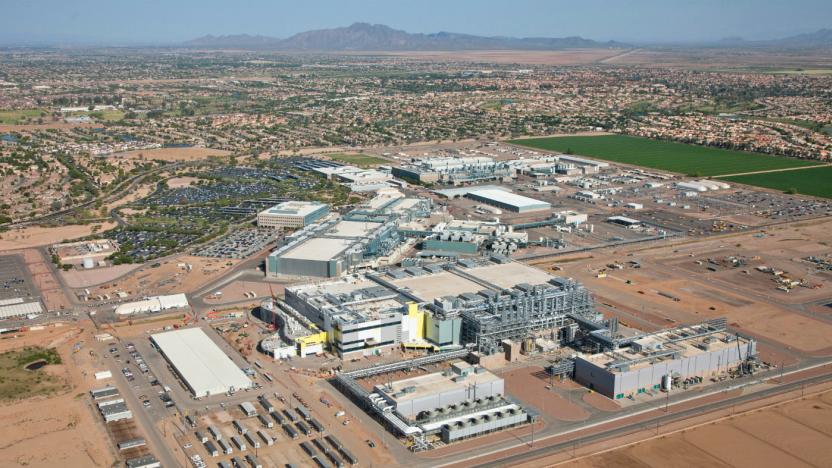
Intel finally plans to finish its Fab 42 factory in Arizona
Intel plans to complete Fab 42, a semiconductor factory in Chandler, Arizona, with an investment of more than $7 billion over the next three to four years. At its peak, the factory will employ about 3,000 process engineers, equipment technicians, and facilities-support engineers and technicians. Fab 42 will produce 7 nanometer chips and is "expected to be the most advanced semiconductor factory in the world" -- whatever that means.

Roadmap says transistors will stop shrinking in 5 years
Whether or not Moore's Law on complexity has always held true, you've had one constant in the semiconductor world: chip makers would always find a way to shrink transistors and create more powerful chips without increasing size or power consumption. However, even that one hint of predictability might soon disappear. The Semiconductor Industry Association (which includes the likes of IBM and Intel) has published a roadmap which expects transistors to stop shrinking after 2021. Simply speaking, it might not be financial practical to keep reducing transistor sizes -- companies might not recoup the costs. Instead, they may focus on 3D chips an other technologies that make better use of available space.

'Plasmonics' could lead to super-fast optic communications
Researchers at Purdue University have developed a new kind of material that could improve the speed of optical communications by as much as 5000 times the current state of the art. The material is made of aluminum-doped zinc oxide (AZO) and it is able to change the amount of light it reflects by up to 40 percent while consuming a fraction of the power that conventional optical semiconductors consume. By reflecting more or less light, the material can encode and transmit data. What's more, this material operates in the near-infrared spectrum range, which is what is most commonly used in optical communications.

'Nano-paper' chips end up in compost heaps, not landfills
Today's cast-off gadgets are far more likely to end up in a landfill than they are being responsibly disposed of. In fact, 41.8 million tons of e-waste were scrapped last year alone. To combat this, a team from the University of Wisconsin-Madison has invented a radically new kind of ecologically-friendly semiconductor chip made from wood. No, seriously.

3D printing technique will put electronics into just about everything
You can use 3D printing to make a handful of electronics, such as antennas and batteries, but LEDs and semiconductors have been elusive; you usually need some other manufacturing technique to make them work, which limits what they can do and where they'll fit. A team of Princeton researchers recently solved this problem, however. They've found a way to make quantum dot LEDs (and thus semiconductors) using only a 3D printer. The scientists choose printable electrodes, polymers and semiconductors, which are dissolved in solvents to keep them from damaging underlying layers during the printing process; after that, the team uses design software to print the materials in interweaving patterns. In this case, the result is a tiny LED that you could print on to (or into) many objects, including those with curved surfaces.

ST-Ericsson joint venture begins dissolution process, 1,600 jobs gone in the process
It's typically a bad sign when a major semiconductor company sees its CEO walk away, and no one in adjoining offices stops to do anything about it. Such is the case with ST-Ericsson, a (now) failed joint venture of STMicroelectronics and Ericsson. The two outfits have seemingly failed to find a suitor for the JV, leaving them with relatively few options -- poor ones at that. In a release posted today (and embedded after the break), the entity has stated that each partner company will take on some of the business, but around 1,600 jobs will be lost from the sectors that neither has interest in. ST-Ericsson was an attempt to jump-start a semiconductor business in Europe, but it actually hasn't turned a profit since forming in 2008. Ericsson will take on the design, development and sales of the LTE multimode thin modem products, including 2G, 3G and 4G multimode, while ST will take on the existing ST-Ericsson products, other than LTE multimode thin modems, and related business as well as certain assembly and test facilities. It's expected that the particulars will clear regulatory hurdles in Q3 of this year, and in order to make sure things go as well as they can in the interim, Carlo Ferro is being appointed president and CEO of the JV starting on April 1st.

IBM Labs develops 'initial step' towards commercial fabrication of carbon nanotubes
Commercialization of carbon nanotubes is one of the holy grails of next-gen computing, and IBM thinks it's made crucial steps toward making this a reality. This isn't the first time that we've heard such a claim, of course, but IBM's considerable resources will make this particularly interesting. The specific problem it's been tackling is placing enough semiconducting nanotubes together to be useful in commercial chips, with current attempts being more in the hundreds, rather than billions that would be required. The new approach uses ion-exchange chemistry that allows controlled placement of nanotubes at two orders of magnitude greater than before, with a density of roughly a billion per square centimeter. To achieve this, the nanotubes are mixed with a soap-like substance that makes them water-soluble. Next, a substrate comprising two oxides and a hafnium oxide "trench" is immersed in the soap-solution, which results in the nanotubes attaching to the hafnium oxide canals with a chemical bond. Simple when you think about it! IBM hopes that as the materials and method are readily accessible now, that industry players will be able to experiment with nanotube technology at a much greater scale. Though, as we've become accustomed, there's no solid timescales on when this might realistically unfold.

New process for nanotube semiconductors could be graphene's ticket to primetime (video)
In many ways, graphene is one of technology's sickest jokes. The tantalizing promise of cheap to produce, efficient to run materials, that could turn the next page in gadget history has always remained frustratingly out of reach. Now, a new process for creating semiconductors grown on graphene could see the super material commercialized in the next five years. Developed at the Norwegian University of Science and Technology, the patented process "bombs" graphene with gallium, which forms droplets, and naturally arranges itself to match graphene's famous hexagonal pattern. Then, arsenic is added to the mix, which enters the droplets and crystallizes at the bottom, creating a stalk. After a few minutes of this process the droplets are raised by the desired height. The new process also does away with the need for a (relatively) thick substrate to grow the nanowire on, making it cheaper, more flexible and transparent. The inventors state that this could be used in flexible and efficient solar cells and light emitting diodes. We say forward the revolution.

Samsung spending $4 billion to renovate Austin chip factory
Premiership footballers will be weeping in envy at the way Samsung's been spending its cash this month. After splashing $822 million on a Korean R&D center, it's now chucking $4 billion to renovate its semiconductor factory in Austin, Texas. The cash will be used to increase production on system-on-chip products used in a wide variety of smartphones and tablets, presumably to cope with future demand. It's not clear if this investment is in addition to the $1 billion it was raising in January to add a new SOC and OLED line to the same facility, but it's certainly a good time to be living in Texas, right now.

IBM creates consistent electron spin inside semiconductors, takes spintronics one twirl closer
A fundamental challenge of developing spintronics, or computing where the rotation of electrons carries instructions and other data rather than the charge, has been getting the electrons to spin for long enough to shuttle data to its destination in the first place. IBM and ETH Zurich claim to be the first achieving that feat by getting the electrons to dance to the same tune. Basing a semiconductor material on gallium arsenide and bringing the temperature to an extremely low -387F, the research duo have created a persistent spin helix that keeps the spin going for the 1.1 nanoseconds it would take a normal 1GHz processor to run through its full cycle, or 30 times longer than before. As impressive as it can be to stretch atomic physics that far, just remember that the theory is some distance from practice: unless you're really keen on running a computer at temperatures just a few hops away from absolute zero, there's work to be done on producing transistors (let alone processors) that safely run in the climate of the family den. Assuming that's within the realm of possibility, though, we could eventually see computers that wring much more performance per watt out of one of the most basic elements of nature.

Researchers make unsuitable parts work as solar cells, could lead to cheaper panels
Harnessing the power of the sun is a tricky business, but even the past few weeks have seen some interesting developments in the field. In this latest installment, researchers from the Lawrence Berkeley National Laboratory and the University of California have figured out a way of making solar cells from any semiconductor, potentially reducing the cost of their production. You see, efficient solar cells require semiconductors to be chemically modified for the current they produce to flow in one direction. The process uses expensive materials and only works with a few types of semiconductors, but the team's looking at using ones which aren't normally suitable -- the magic is to apply an electrical field to them. This field requires energy, but what's consumed is said to be a tiny fraction of what the cell's capable of producing when active, and it means chemical modification isn't needed. The concept of using a field to standardize the flow of juice isn't a new one, but the team's work on the geometrical structure of the cells has made it a reality, with a couple of working prototypes to satisfy the skeptics. More of these are on the way, as their focus has shifted to which semiconductors can offer the best efficiency at the lowest cost. And when the researchers have answered that question, there's nothing left to do but get cracking on commercial production. For the full scientific explanation, hit up the links below.

Samsung swallows up CSR mobile and location patents for $310 million
The S-Wallet has opened and absorbed $310 million-worth of connectivity and location patents from British chip company CSR, which already supplies SiRF GPS chips to Galaxy devices. In addition to boosting its patent portfolio, Samsung also invested $34 million to buy a five percent stake in the firm itself, giving it access to a large development team working on audio, automotive, indoor location and other functions. The deal won't let Samsung use CSR's camera technology, but it will -- the Korean manufacturer says -- "solidify its position as a leading semiconductor solutions provider." Given how Sammy is already intent going it alone with its Exynos processors, we have no reason to doubt it.

Intel to buy 15 percent of silicon fab equipment maker ASML, wants manufacturing machines made faster
Chipzilla didn't get its position as the king of semiconductors by twiddling its thumbs, folks. It became a Valley behemoth by delivering us faster and better silicon, and its latest $4.1 billion purchase -- a 15 percent stake in silicon manufacturing equipment maker ASML Holding NV -- should help keep Intel atop the CPU heap. You see, Intel's in the process of retooling its chip manufacturing process to use bigger diameter silicon wafers, which'll make those Ivy Bridge, ValleyView and other future chips cheaper for all of us. Such retooling can take years to implement, which is likely why Intel was willing to plunk down so much cash to ensure nothing futzes with its manufacturing timetable. The company's investment will presumably give it the clout to get ASML's crucial lithography equipment on the fast track to completion. Hop to it, fellas, we want our CPUs at bargain-basement prices, and we want them now.


