1
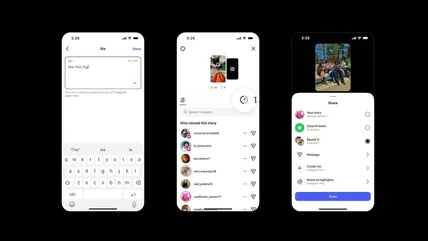
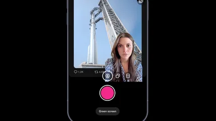
Wired found code for an unreleased facial recognition feature in Meta's AI app
Meta was previously reported to be exploring facial recognition for its smart glasses.
Read More
Meta was previously reported to be exploring facial recognition for its smart glasses.
Read MorePaying users will have tools for reaching either wider or more-specific audiences.
Read MoreOpenAI has significantly improved the chatbot's "dreaming" architecture.
Read MoreCanada's "AI for All" plan prioritizes strengthening data protections and increasing AI adoption.
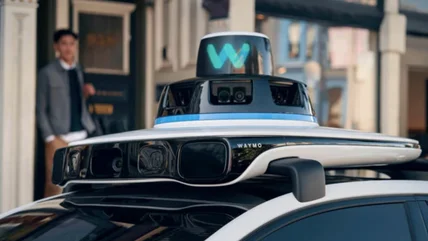
Read MoreBelieve it or not, this is not the first robotaxi-assisted theft.
Read MoreOnly 4,999 units of the HP Scuderia Ferrari AI PC will be available.
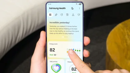
Read MoreSamsung will roll out an update for its Health app before launching its new Galaxy Watches.
Read MoreThe group has "due process concerns" over how the company handles account bans.
Read MoreSpaceX expects to become a trillion-dollar company when it goes public.
Read MoreNoble's FoKus Artemis headphones have three drivers and ANC, but they don't come cheap.
Read MoreThe flagship OpenDots 2 earbuds are joined by the mid-range OpenDots Air.
Read MoreThe state law governing app use by minors takes effect tomorrow.
Read MoreA new Supernatural VR workout app arrives this fall months before Meta planned to shut it down.
Read MoreWiiM, a company known for its lineup of speakers and amplifiers, has revealed its first soundbar.
Read MoreMark Zuckerberg wants agents to be able to "run your whole business."
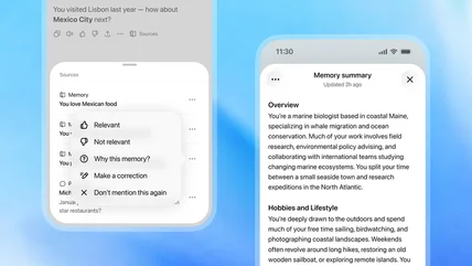
Read MoreMaking sense of what you get from Claude AI at the free tier, especially as limits are vague and keep shifting.
Read MoreThe company says opting out won't impact placement in regular searches.
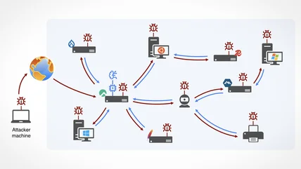
Read MoreResearchers created an AI-powered worm that that can spread through networks with no human intervention.
Read MoreThe Polish government has approved several bills, including one that would ban phones in the classroom.
Read MoreWorkers can pause the all-seeing eye when they need to "check something personal."
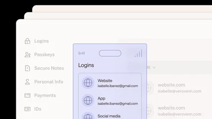
Read MoreHackers used brute forced about 20 password vaults from Dashlane.
Read MoreThe company demoed Solara on an Echo Show-style smart display and a smart key badge.
Read MoreGoogle Photos and Google Play Books are also getting new AI-powered updates.
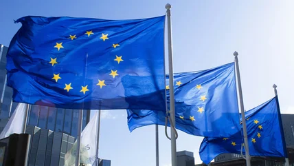
Read MoreThe EU's moves towards digital sovereignty might include its Parliament ditching Google.
Read MoreThe Camp Snap 2 is a slight improvement on the nostalgic throwback camera.
Read MoreTikTok-style superimposed reaction videos are coming to X now.
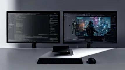
Read MoreMicrosoft is making a Surface AI dev desktop for people who don't want a laptop.
Read More